


essence
-
The monovalent copper ion compounds, which are p-type semiconductors, have faced the problem of the difficulty of controlling the hole concentration.
-
We found that doping with equivalent and bulk alkaline ions is effective in increasing the crater concentration, and we elucidated the mechanism through theoretical calculations.
-
By this method, a p-type semiconductor thin film with high hole concentration and high mobility can be prepared from solution, and it is expected to improve the performance of solar cells.
Summary
He was specially appointed Assistant Professor Kosuke Matsuzaki (at the time of the research, now a Senior Researcher at the National Institute of Advanced Industrial Science and Technology) at the Elements Strategy Research Center, Tokyo Institute of Technology; Professor Emeritus Hideo Hosono; At the time of research, currently: program-specific professor, and concurrent professor at Tohoku University), Professor Fumiyasu Ohba, and graduate student Naoki Tsunoda, in collaboration with Associate Professor Kenji Nomura of the University of California, San Diego.pit transmission materials[用語1]We have developed a doping method using equivalent impurities to improve performance.
A high-performance p-type semiconductor is required for light-absorbing layers and hole-transport materials used in solar cells, and in recent years, monovalent copper-ion compounds have been investigated as candidates. The process of activating holes is important for improving the conversion efficiency, and traditional methods have used ions with a valency lower than the constituent atoms as impurities. However, since there are no ions of lower valency (zero valency) than monovalent copper ions, a hole-activation technique for copper compounds has not been established. In size, effective in increasing the focus of the hole.First principles accounts[用語2]showed that a complex defect formed by combining the voids of added alkaline ions and copper ions becomes a source of holes (electron acceptors). This allows the use of equivalent impurities to achieve a high hole concentration andHole navigation[用語3]Since it is possible to prepare a thin film of p-type copper iodide by the plating method,perovskite solar cell[用語4]It is expected to be applied to high performance hole transfer layers such as
The results of the research were published in the Journal of the American Chemical SocietyJournal of the American Chemical Society(Journal of the American Chemical Society) “published September 1st in electronic publication.
my knowledge
Perovskite solar cells that can be formed at lower temperatures are crystalline Si andsig[用語5]As a next-generation solar cell alongside CdTe, several studies are being conducted. However, many problems still have to be overcome for the practical use of perovskite solar cells. One is the development of a new hole-transport layer (p-type semiconductor) that carries photo-generated holes to the electrode. In organic semiconductors, which have been used as p-type semiconductors, hole impurities degrade the power generation layer and become a factor in reducing the stability of solar cells. On the other hand, chemically stable p-type semiconductors have been proposed as candidate materials to replace organic semiconductors, but their manufacture requires high-temperature heat treatment. Based on the above, expectations are high for the development of inorganic p-type semiconductors that can be synthesized at lower temperatures and have excellent hole-transporting properties.
In this study, the research group focused on copper iodide (CuI), which is a broad-gap inorganic p-type semiconductor that is chemically stable and can be formed into thin films relatively easily using the solution method. However, pure CuI has a hole concentration of 1014−1016 cm−3The development of doping with controllable impurities at higher concentrations was necessary to improve the crater transport properties. Conventional hole activation methods are implemented by replacing ions with lower valences of the constituent cations, such as replacing divalent magnesium ions with trivalent gallium ions in gallium nitride. However, in CuI, which consists of monovalent copper ions, it is necessary to perform the replacement with zero-valent ions, but by definition there are no zero-valent ions, so fossil doping of CuI was considered impossible.
Therefore, copper oxide (Cu2O) and has been experimentally used as a doping agent for CIGSAlkaline impurity effect[用語6]We aimed to propose a new doping design by elucidating the mechanism of hole generation and developing the hole doping technique for CuI.
research results
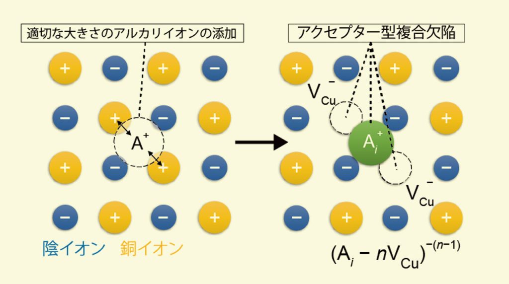
In order to develop a general-purpose doping method for monovalent copper semiconductors, the research group examined copper2By focusing on O, we attempted to elucidate the mechanism by which the host copper ion and equivalent sodium impurities increase the hole concentration (Fig. 1a). P type copper2It is known that in O semiconductors, the vacancies resulting from the removal of Cu ions form acceptor levels that provide holes, resulting in p-type conduction. From the analysis of the first principles account, sodium inclusions are present in the interstitial spaces of the network (interstitial sites). complex defects (NaI-2 voltscopper; Figure 1b). Theoretical analysis revealed that a complex defect consisting of one donor-type defect (interstitial sodium) and two acceptor-type defects (copper vacancies) act as acceptor. In addition, it was confirmed that complex defects act more effectively as a hole denatured because the receptor plane is less deep than the vacancy of copper ions. From the complex defect structure, it is inferred that the electrostatic repulsion between monovalent sodium ions and monovalent copper ions is the driving force, and adjacent copper ions escape from the original lattice sites to generate vacancies. In addition, sodium ions have a larger ionic radius than copper ions, and are more stable when combined with more neighboring anions.
Based on the above results, even in CuI, where copper vacancies are the origin of the p-type conduction, the electrostatic repulsion between the impurity cations and the copper ions causes many copper ions to escape from a single impurity, resulting in the presence of vacancies. (Fig. 1c), which leads to an improvement in the hole focus. Also, copper2Based on the results of investigations with O, it was concluded that the size of the alkaline ions to be added is important in the formation and stabilization of holes. In other words, if the inclusions are small enough relative to the size of the interstitial gap, the cation will act as a donor by being placed between the lattices, while if it is large enough, the impurities will not enter the lattice. Therefore, in order to form complex defects of the future type that provide holes, it is necessary to select fairly large inclusions according to the crystal structure.
Figure 1. copper2Doping perforation with Na impurities from O and its doping motif.
(a) with2Hole concentration and hole motion in O:Na and single crystals. (b) A complex defect of the acceptor type (Na .).I-2 voltscopper) structure. (c) Equivalent impurities+copper ion+Model of complex defects resulting from electrostatic repulsion with ions. Benny A+and the neighboring Cu+The vacancies and copper (V.copper).
In this study, the research group investigated the potassium, rubidium and cesium among the alkali metals as doping impurities of CuI, which contains large voids. As a result, the hole concentration (1014−1016 cm−3from 1017−1019 cm−3; Figure 2a) It was successfully controlled. In addition, the coating method uses a solution as a raw material, and the orifice concentration is 10%.19 cm−3Thus the kinematics (1-4 cm2/Vs) (Fig. 2a). When the defect structure of cesium impurities was analyzed by the method of theoretical calculation, CsI-3 voltscopper−VIand CsI-4 voltscopper−VIIt was found that the added cesium stabilizes the complex defect consisting of multiple copper ion vacancies and iodine vacancies, both of which formed shallow acceptor levels (Fig. 2b). Cesium impurities in such copper is copper2Similar to the sodium impurity in O, due to the electrostatic repulsion between cations of the same valence, a acceptor-type complex defect consisting of multiple copper ion vacancies acts as an impurity for a single impurity.
These results demonstrate that, in contrast to the traditional doping method in which ions of different valences are replaced by ions that make up the matrix, impurities with the same valence ions of different sizes can form shallow receptive levels.

Figure 2. Doping perforation of CuI using Cs impurities.
(a) Hole concentration and hole mobility in CuI: aggregated Cs single crystals and solution-treated polycrystalline thin films. (b) cI-3 voltscopper−VIOne acceptor and CsI-4 voltscopper−VIComplex defect structure of the double acceptor.
social impact
The hole-doping method developed in this paper is a core technology widely used in semiconductor devices, and is expected to improve the performance of solar cells, especially those containing p-type semiconductors. In addition, elucidation of the mechanism of doping in monovalent copper semiconductors by alkaline impurities may contribute to elucidating the role of alkaline impurities, which is essential for improving the performance of CIGS solar cells, which has yet to be elucidated.
next post
This result made it possible to fabricate a high-capacity inorganic p-type semiconductor in a simple way using a low-temperature solution as a raw material. The method is expected to be applied to inorganic hole transport layers such as perovskite solar cells, which require robustness.
Supplementary Note
The results of this research are Ministry of Education, Culture, Sports, Science and Technology Elements Strategy Project (Basic Formation Type) (No. JPMXP0112101001), Research Center Formation Program (JPJSCCA20180006), Grants in Aid for Scientific Research (No JP22K19094, JP19H02427, JP20J21608, JP20H00302), implemented with the support From the Murata Foundation for the Advancement of Science.
Glossary of terms
[用語1]
pit transmission materials : A material that selectively transmits holes (positive charges) and electrons (negative charges) generated in the photovoltaic layer of a solar cell by absorbing light energy to the outer electrode. In perovskite solar cells and thin-film organic solar cells, organic p-type semiconductors, which can be made at lower temperatures, are often used as the hole transfer layers. In general purpose organic hole transfer materials, hygroscopic additives that provide high hole transfer properties degrade the power generation layer and reduce its durability.
[用語2]
First principles accounts : Calculations based on the basic principles of quantum mechanics. By numerically calculating the state of electrons that govern the properties of matter, we can obtain the energy and forces acting on atoms, and use them to predict the structure and stability of crystals and molecules.
[用語3]
Hole navigation A physical quantity that indicates the ease with which holes can move in a material. Mobility is an important indicator that determines the properties of semiconductor devices. In a solar cell, the higher the mobility, the easier it is to move the holes, which leads to higher photoelectric conversion efficiency.
[用語4]
perovskite solar cell : A solar cell with a perovskite halide crystal composed of organic and inorganic elements as a power generation layer, and it has been extensively studied in recent years. It has a sandwiched structure between the electron transport layer, hole transport layer, and external electron-extracting electrodes and holes on either side of the perovskite power generation layer.
[用語5]
CIGS solar cells : Monovalent p-type multicomponent Cu (In, Ga) Se composed of copper, indium, gallium, selenium and sulfur2 (CIGS) Thin-film solar cells as a layer for power generation.
[用語6]
Alkaline impurity effect : In CIGS solar cells, the addition of alkaline impurities such as sodium increases the hole concentration and greatly improves the photoelectric conversion efficiency. The mechanism remained unclear for more than 20 years.
paper information
|
Posted in: |
Journal of the American Chemical Society |
|
Paper title: |
Puncture doping to a copper(I)-based semiconductor with an isoelectric cation: use of a complex defect as a shallow acceptor. |
|
Author: |
Kosuke Matsuzaki, Naoki Tsunoda, Yu Kumagai, Yalun Tang, Kenji Nomura, Fumiyasu Oba, Hideo Hosono |
|
DOI: |

“Travel maven. Beer expert. Subtly charming alcohol fan. Internet junkie. Avid bacon scholar.”
More Stories
Sleep without your iPhone alarm going off! ? Causes and Countermeasures to Wake Up with Peace of Mind – iPhone Mania
A close-up image of the dark nebula “Horsehead Nebula” observed by the Webb Space Telescope |
Hasbro, which has had huge success with “Baldur's Gate 3” and “MONOPOLY GO!”, is developing a $1 billion in-house video game “doope!” Local and international gaming information website